
The Invisible Brain of the World: Semiconductor Solutions for Academic Leadership and Research Excellence
Semiconductor solutions are central to strengthening academic ecosystems by enabling advanced teaching, high-impact research, and industry collaboration. For institutional leaders, these solutions provide the tools and platforms necessary to drive innovation and maintain global academic competitiveness

An FPGA (Field Programmable Gate Array) Laboratory equipped with industry-standard Electronic Design Automation (EDA) tools is essential for modern engineering education and research. Tools such as Questa and ModelSim from Siemens EDA, provide a comprehensive environment for digital design, simulation, and verification.
This lab enables students and researchers to design, simulate, and validate digital systems before hardware implementation, aligning academic training with industry practices.
Download PDF
An Application-Specific Integrated Circuit (ASIC) Laboratory is a cornerstone facility for advanced semiconductor education and research. By integrating industry-standard EDA tools such as Tanner EDA, Calibre, Aprisa, Catapult, and Symphony from Siemens EDA, institutions can establish a complete end-to-end ASIC design ecosystem.
This lab supports the full chip design flow — from specification and modeling to layout, verification, and tape-out readiness.
Download PDF
A Printed Circuit Board (PCB) Laboratory is a fundamental facility for electronics design, bridging circuit theory with real-world hardware implementation. By integrating advanced EDA tools such as Analog FastSPICE, PADS, and HyperLynx from Siemens EDA, institutions can establish a complete PCB design, simulation, and validation ecosystem.
This lab enables students and researchers to design, simulate, analyze, and prototype high-performance electronic systems with industry-standard workflows.
Download PDF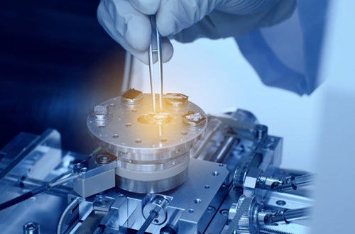
A Technology Computer-Aided Design (TCAD) Laboratory is essential for advanced semiconductor device research and modeling. TCAD tools enable simulation of semiconductor fabrication processes and device behavior at the physics level, eliminating the need for costly fabrication in early research stages.
Using solutions from Silvaco, institutions can establish a powerful simulation-driven research environment for device engineering, process optimization, and next-generation semiconductor development.
Download PDF
An Embedded Systems and VLSI Laboratory forms the backbone of modern electronics and semiconductor education. By integrating industry-aligned platforms and training ecosystems from LinkedLoop, academic institutions can deliver a holistic learning experience that bridges hardware design, software development, and chip-level engineering.
This lab enables students and researchers to design intelligent systems — from microcontroller-based applications to complex VLSI architectures — ensuring alignment with current industry standards.
Download PDFProvide students and researchers access to industry-standard EDA tools and real-world semiconductor workflows.
Enable complete chip design workflows from concept to validation across FPGA, ASIC, PCB, and VLSI domains.
Support integrated research across electronics, embedded systems, semiconductor physics, and system-level design.
Strengthen institutional capability for funded research, IP creation, and high-impact technical publications.
Align academic infrastructure with India Semiconductor Mission (ISM) and global semiconductor development goals.
Develop industry-ready graduates skilled in VLSI, embedded systems, and semiconductor technologies.
Build scalable labs and centers of excellence for emerging technologies like AI hardware and advanced chip design.
Transform your department into a center of excellence for next-generation electronics and semiconductor innovation with Siemens EDA, Silvaco & LinkedLoop powered lab ecosystems.
